
ICT-2010-257964
NANO-TEC: Ecosystems Technology and Design for Nanoelectronics
Authors: Clivia Marfa Sotomayor Torres, FUNDACIO INSTITUT CATALA D...; Jouni Ahopelto, Teknologian tutkimuskeskus VTT Oy, FI; ; Ralf Popp, edacentrum GmbH, DE;
NANO-TEC showed first results, but there are still things to be done …
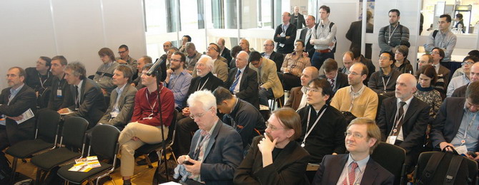
Especially in the Beyond CMOS area the interaction between the research communities of design and technology is characterized by a diversity of terminologies, modes of operation and the absence of a consensus on main priorities. Therefore the NANO-TEC project aims to bring together these communities for the benefit of a stronger European Research Area in future. To achieve this goal the project organizes a series of four workshops to elaborate their findings from identification over benchmarking and an analysis
on the strengths, weaknesses, opportunities and threats (SWOT analysis) up to recommendations. These workshops are flanked by a website with different networking functions to stimulate and support the scientific exchange, in particular on the workshops content and results.
This article contains an introduction to the EU project NANO-TEC and its findings up to the third workshop on SWOT analysis, which meanwhile took place in the end of May in Lausanne, Switzerland. It includes a summary of the – for the NANO-TEC project – most promising technology trends. Further on it shows a preliminary benchmarking analysis for some of these trends as an example of the project work. Additionally relevant design issues concerning these technologies are summarised followed by conclusions
and recommendations to bridge this design-technology gap.
Publication Date: 2012/07/12
Location of Publication: newsletter edacentrum 01 2012, ISSN 1862 2283, July 2012
Keywords: Nanoelectronics; Semiconductors; Research/Education
Download(s):

