
ICT-2010-257964
SWOT Analysis of the Technology Design Ecosystem
Author: Ralf Popp, edacentrum GmbH, DE
Report on a panel at the 3rd NANO-TEC Workshop
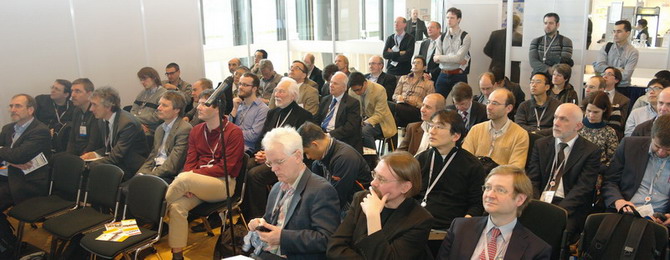
The project NANO-TEC (“ECOSYSTEMS TECHNOLOGY and DESIGN for NANOELECTRONICS”) organizes a series of workshops in order to establish a joint Design-Technology Community for Nanoelectronics in Europe. During the 1st NANO-TEC workshop in January 2011 the requirements for future ‘Beyond CMOS’ devices have been identified. These devices have been benchmarked during the 2nd workshop in October 2011. The objective of the 3rd workshop in May 2012 was to conduct an analysis on the strength, weaknesses, opportunities and threats (SWOT analysis) of the benchmarked devices. This analysis took into account the technology and design aspects, but also application perspectives. The target outcome of the workshop was a number of exploitation scenarios for selected number of ‘Beyond CMOS’ devices. As the detailed documentation of the workshop is currently set up, this article gives only a short overview on the workshop. Additionally it provides a report of the panel session, which took place at the end of the workshop.
Publication Date: 2012/07/12
Location of Publication: newsletter edacentrum 01 2012, ISSN 1862 2283, July 2012
Keywords: Nanoelectronics; Semiconductors; Research/Education
Download(s):

