
ICT-2010-257964
Session 2 - Molecular Electronics
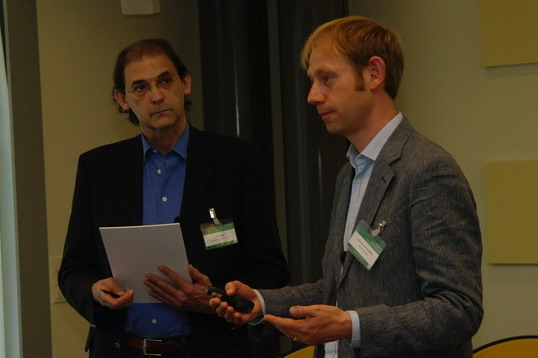 | |
Presenter: Sense van der Molen, Leiden University | Discussion on Molecular Electronics led by Paolo Lugli, TU München |
Download presentaition on Melecular Electronics
SENSE JAN VAN DER MOLEN, Leiden University
He studied physics in Groningen, Netherlands, following an exchange year in Olympia, Washington, USA. My Masters project, carried out under prof. Teun Klapwijk, focused on quantum mechanical interference effects in mesoscopic samples. Next, he moved to the group of prof. Ronald Griessen at the Vrije Universiteit, Amsterdam. Here, he investigated so-called switchable mirrors. These metalhydrides, e.g. YHx, switch from perfect mirrors to transparent windows upon hydrogen uptake. His work focused on both the fundamentals of the metal-insulator transition and the possibility to manipulate the hydrogen concentration in these mirrors electrically (e.g. by electromigration). In 2002, he joined the group of prof. Bart van Wees, to start up a new research line in molecular transport (Groningen, the Netherlands). They put considerable effort in creating and optimizing new techniques to investigate single molecules. In a collaboration with prof. Ben Feringa, they focused on light-sensitive, switchable molecular devices. Furthermore, they explored the exciting field of spin transport through carbon nanotubes. In 2005, he obtained an NWO talent grant to perform research in the group of Christian Schönenberger (Basel, Switzerland). Later he moved to Leiden in 2007, to take up the challenge of building up my own research group. He is the project leader of 'ESCHER' for which they recently obtained a large 'NWO-groot onderzoek' grant. They aim at using aberration-corrected LEEM/PEEM (resolution down to 2 nm) to study fascinating phenomena in nanoscience. For this he collaborates with prof. Ruud Tromp (Leiden and IBM Yorktown) and others. Their first attempts to apply a Medipix 2 detector to LEEM/PEEM have proven very successful. In November 2009, he received a VIDI-grant for research on molecular transport using the best of the properties of LEEM and PEEM. He is working on this research program at the Leiden Center for Ultramicroscopy (LCU), which we established on September 17, 2010. Together with Peter Liljeroth, he recently wrote a review on charge transport through molecular switches.
Abstract:
Molecular electronics: How to get the most out of molecular functionality?
The most appealing property of molecular electronics is the versatility offered by the chemical diversity of molecules suitable for electronic device purposes. In contrast to silicon-based devices, molecules can be synthesized with built-in functionality such as switching, rectification behaviour, molecular sensing or magnetism. This versatility combined with the cheap fabrication methods available for soluble molecular systems (printing, self-assembly, etc.) is the driving force behind the field. The fact that charge transport is dominated by quantum effects, even at room temperature, makes this area of nanoscience even more fascinating.
During the last years different techniques have become available to study charge transport through (functional) molecules. These can be generally divided in two types of devices, which have in common that the basic unit is always a metal-molecule-metal junction. On the one hand there are single molecular devices (both two-terminal and three-terminal, i.e. with gate). These are used to fundamentally study molecular conductance properties, mostly at low temperatures. Then there are multimolecular devices, which are generally created by self-assembly techniques. Such devices combine a relatively good stability in the ambient (up to weeks, but not years) with the possibility to explore molecular functionality, such as switchability and rectification. For some device choices, molecular functionality can even be enhanced!
By now it is clear that molecular electronics will not provide a basis to replace CMOS technology. However, applications in which specific molecular functionalities (e.g. (bio) sensing, switching) are combined with CMOS technology are to be explored. It will be key to control self-assembly and interfacing in such structures. Other nano-objects (wires, particles) may be used to bridge the size gaps. To explore new functionalities and to further sharpen our knowledge on molecular charge transport fundamental research at the single molecular level remains of great importance. It is expected that also the field of organic electronics (OLEDS, photovoltaics) will profit from these insights.
